












For many professionals, an engineering degree and international work experience is everything. But Shweta Suman chose another journey; the journey took a different turn. After studying engineering, spending time in Oman and gaining professional experience, she came back to Bihar after marriage. Instead of treating the move as a reason to put her ambitions on hold, she chose to build a technology business.Meet Shweta SumanMeet Shweta Suman, who is the founder of Swadeza, a Bihar-based technology company. It works on artificial intelligence-powered tools for semiconductor engineering. In September 2026, the startup took another significant step when it showcased its semiconductor technology at SEMICON India 2026 in New Delhi, placing a firm built from Bihar in the spotlight of India’s growing semiconductor ecosystem.From Oman to BiharSuman’s journey started in Oman, where she attended school. She later pursued engineering at Birla Institute of Technology (BIT), Mesra, before returning to Oman. Eventually, after marriage, she moved back to Bihar.After being back, she began developing Swadeza as a company with multiple areas of work, including semiconductor technology, IT consulting and development, and digital marketing.The company’s growing focus, however, is on deep technology, particularly the use of AI to simplify some of the complex engineering processes involved in designing chips.Why semiconductor design needs AISemiconductor manufacturing often receives attention because of the huge investments required to establish fabrication facilities. But before a chip can be manufactured, it must pass through several demanding stages of design, testing and verification.Engineers need to ensure that every component of a chip functions according to its specifications. This process, known as design verification, can be time-consuming. Identifying an error after a chip has moved to manufacturing can also prove expensive.This is the problem Swadeza is attempting to address through its AI-native semiconductor engineering platform, FORGE.Rather than functioning like a general-purpose AI chatbot, the platform is designed to understand the architecture of a chip and provide engineers with relevant information for specific tasks. It creates a structured map of the chip and uses relevant portions of that information to answer engineering queries and support design workflows.FORGE: Building tools for the chip-design process
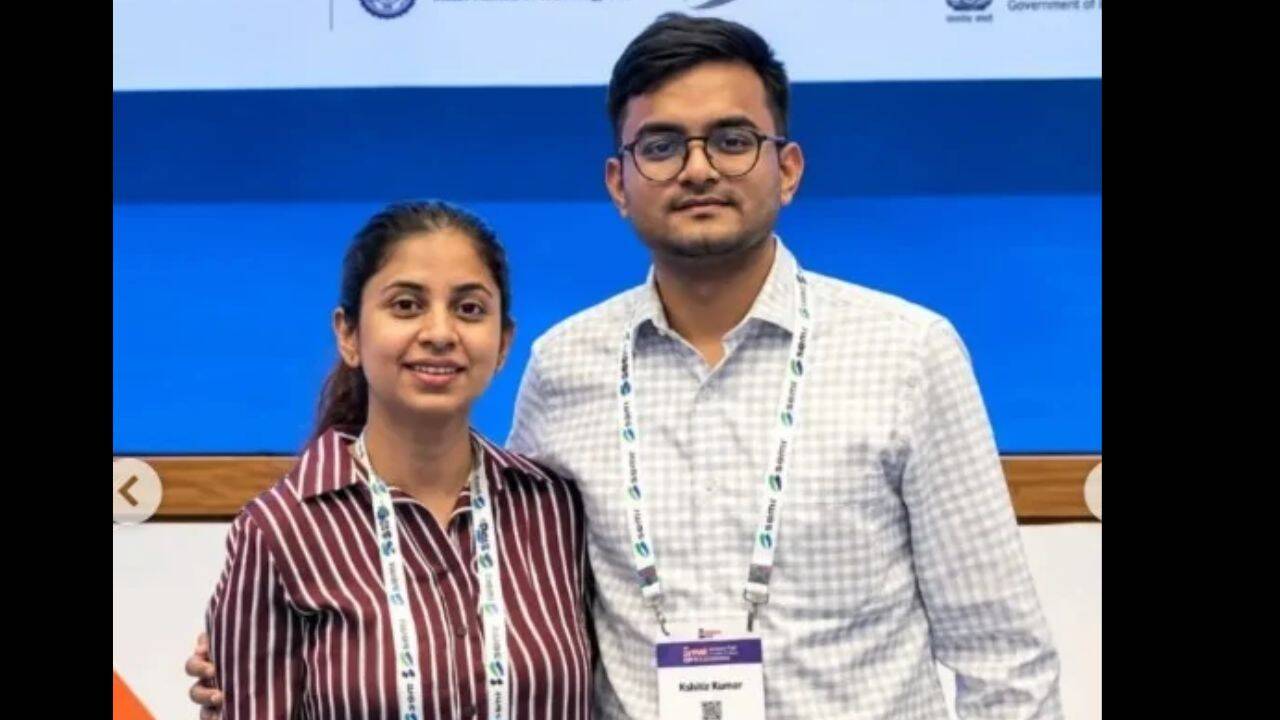
Shweta Suman
Swadeza’s FORGE platform is being developed around four specialised tools, each targeting a different stage of the semiconductor lifecycle. Its first product, DV-FORGE, focuses on design verification. It can read a chip’s reference manual and generate verification plans, coverage models and Universal Verification Methodology (UVM) testbenches.According to the company, the technology was used on OpenTitan-class system-on-chips (SoCs). Swadeza says it completed verification sign-off for OpenTitan Earlgrey in 30 days and identified seven bugs across approximately 40 intellectual property blocks and 2,581 registers. Its derivative, Darjeeling, was signed off in 21 days.The company also claims that its approach uses 80% fewer tokens than a conventional AI assistant.Another product, PD-FORGE, is being developed to help engineers identify and trace physical-design violations to the stages that caused them. Two additional tools, PS-FORGE and SC-FORGE, are aimed at post-silicon validation and standard-cell optimisation and remain under development.Taking a Bihar-built startup to the national stageThe opportunity to showcase FORGE at SEMICON India 2026 marked an important milestone for Suman and her team. The fifth edition of the event was held at Yashobhoomi, New Delhi, from September 17 to 19, bringing together more than 600 exhibiting companies and representatives from 52 countries.The exhibition featured industry leaders, research institutions, startups and policymakers working across the semiconductor value chain.Swadeza made its first public demonstration of FORGE at startup pod 6. The company also featured in Forbes India’s photographic coverage of the event, alongside established names such as IBM and Tata Electronics, according to its account published by YourStory.For a startup operating from Bihar, the opportunity was significant. It demonstrated that companies working on sophisticated technology need not necessarily originate from Bengaluru, Hyderabad, Pune or other established technology centres.A changing landscape for BiharSuman’s entrepreneurial journey also comes at a time when Bihar is attempting to establish a presence in India’s semiconductor industry.In January 2026, the Bihar government published its Semiconductor Policy 2026, outlining the state’s ambitions to attract investment in the sector. The policy is part of a broader effort to bring technology-driven industries and employment opportunities to the state.At the national level, the Union Cabinet approved Semicon 2.0 in July 2026 with an outlay of ₹1,27,500 crore. The programme aims to strengthen India’s semiconductor ecosystem through support for chip design, manufacturing, research, equipment, materials and talent development.Swadeza’s approach represents a different aspect of this ambition. Instead of setting up a fabrication facility, it is concentrating on the engineering software and tools that can help semiconductor companies design, test and improve chips.The company is also working with professors from BIT Patna and Signitude, a fabless semiconductor company, as part of its technology development efforts.There are still challenges ahead. PD-FORGE is undergoing closed testing, while its post-silicon validation and standard-cell products are under development. The company’s next steps include taking its tools towards wider commercial adoption and converting industry interest into customer deployments.Her journey from studying engineering in Oman and India to returning to Bihar and showcasing an AI-powered semiconductor platform at a major industry event is a reminder that innovation does not always follow the usual geographical map.And perhaps that is what makes her story stand out: she did not simply return to Bihar; she returned with an ambition to build something that could put the state on a very different technology map.